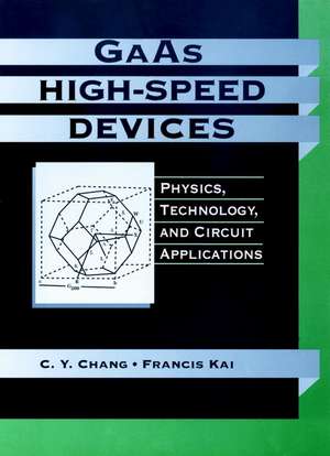
Speed Devices
Autor Chang, Kaien Limba Engleză Hardback – 16 sep 1994
Beginning with chapter 2 of part one, the book discusses such basic subjects as gallium arsenide materials and crystal properties, electron energy band structures, hole and electron transport, crystal growth of GaAs from the melt and defect density analysis. Part two describes the fabrication process of gallium arsenide devices and integrated circuits, shedding light, in chapter 3, on epitaxial growth processes, molecular beam epitaxy, and metal organic chemical vapor deposition techniques. Chapter 4 provides an introduction to wafer cleaning techniques and environment control, wet etching methods and chemicals, and dry etching systems, including reactive ion etching, focused ion beam, and laser assisted methods. Chapter 5 provides a clear overview of photolithography and nonoptical lithography techniques that include electron beam, x-ray, and ion beam lithography systems. The advances in fabrication techniques described in previous chapters necessitate an examination of low-dimension device physics, which is carried on in detail in chapter 6 of part three.
Part four includes a discussion of innovative device design and operating principles which deepens and elaborates the ideas introduced in chapter 1. Key areas such as metal-semiconductor contact systems, Schottky Barrier and ohmic contact formation and reliability studies are examined in chapter 7. A detailed discussion of metal semiconductor field-effect transistors, the fabrication technology, and models and parameter extraction for device analyses occurs in chapter 8. The fifth part of the book progresses to an up-to-date discussion of heterostructure field-effect (HEMT in chapter 9), potential-effect (HBT in chapter 10), and quantum-effect devices (chapters 11 and 12), all of which are certain to have a major impact on high-speed integrated circuits and optoelectronic integrated circuit (OEIC) applications.
Every facet of GaAs device technology is placed firmly in a historical context, allowing readers to see instantly the significant developmental changes that have shaped it. Featuring a look at devices still under development and device structures not yet found in the literature, GaAs High-Speed Devices also provides a valuable glimpse into the newest innovations at the center of the latest GaAs technology. An essential text for electrical engineers, materials scientists, physicists, and students, GaAs High-Speed Devices offers the first comprehensive and up-to-date look at these formidable 21st century tools.
The unique physical and electrical properties of gallium arsenide has revolutionized the hardware essential to digital computers, advanced electronic systems for digital signal processing, telecommunication systems, and optoelectronics. GaAs High-Speed Devices provides the first fully comprehensive look at the enormous range of engineering devices gallium arsenide has made possible as well as the backbone of the technology--ication methods, operating principles, and the materials properties and physics of GaAs--device models and novel device designs. Featuring a clear, six-part format, the book covers:
- GaAs materials and crystal properties
- Fabrication processes of GaAs devices and integrated circuits
- Electron beam, x-ray, and ion beam lithography systems
- Metal-semiconductor contact systems
- Heterostructure field-effect, potential-effect, and quantum-effect devices
- GaAs Microwave Monolithic Integrated Circuits and Digital Integrated Circuits
Preț: 1762.88 lei
Preț vechi: 2414.90 lei
-27%
Puncte Express: 2644
Carte tipărită la comandă
Livrare economică 26 noiembrie-10 decembrie
Livrare prin curier în România Termenul estimat este afișat lângă disponibilitate.
Transport gratuit pentru acest produs Plată online sau ramburs, în funcție de opțiunile comenzii.
Retur gratuit în 14 zile Comandă securizată și suport în română.
Specificații
ISBN-13: 9780471856412
ISBN-10: 047185641X
Pagini: 632
Dimensiuni: 183 x 260 x 38 mm
Greutate: 1.1 kg
Editura: Wiley
Locul publicării:Hoboken, United States
ISBN-10: 047185641X
Pagini: 632
Dimensiuni: 183 x 260 x 38 mm
Greutate: 1.1 kg
Editura: Wiley
Locul publicării:Hoboken, United States
V-ar putea interesa
-
 ULSI DevicesChang-9%Preț: 1470.78 lei1616.25 lei
 -
 Preț: 382.65 lei
 -
 -18%Preț: 779.10 lei950.12 lei
 -
 -15%Preț: 650.55 lei765.35 lei
 -
 Bio-inspired Structured AdhesivesLars Heepe-24%Preț: 900.98 lei1185.49 lei
 -
 CarbonTapan Gupta-24%Preț: 882.27 lei1160.88 lei
 -
 -24%Preț: 1127.67 lei1483.78 lei
 -
 Advances in Materials and MetallurgyA. K. Lakshminarayanan-24%Preț: 930.78 lei1224.71 lei
 -
 -15%Preț: 659.97 lei776.43 lei
 -
 -15%Preț: 609.73 lei717.34 lei
 -
 -24%Preț: 1168.85 lei1537.96 lei
 -
 -15%Preț: 613.81 lei722.13 lei
 -
 Composite Materials Engineering, Volume 2Xiao-Su Yi-18%Preț: 1516.94 lei1849.93 lei
 -
 -24%Preț: 1314.02 lei1728.97 lei
 -
 ELECTROMAGNETIC MATERIALSHock Lim-18%Preț: 1052.70 lei1283.78 lei
Notă biografică
C. Y. CHANG is Professor and Dean of the College of Engineering atNational Chiao Tung University, Taiwan. He is also the Director ofthe National Nano Device Laboratory. Dr. Chang was elected a fellowof the IEEE in 1988 for his "contributions to semiconductor devicedevelopment and to education."
FRANCIS KAI is an Analytical Tools Engineer at Dell ComputerCorporation. He formerly served as a Senior Systems Engineer atCreative Applications, Inc., Senior Engineer at Compaq ComputerCorporation, and Assistant Professor at Northeastern University.Dr. Kai earned his PhD in solid state electronics from the StateUniversity of New York at Buffalo. He has varied experience insemiconductor processing, high-speed device design, devicemodeling, VLSI circuit design, signal integrity and electromagneticcompatibility, software development, and medical imaging.
FRANCIS KAI is an Analytical Tools Engineer at Dell ComputerCorporation. He formerly served as a Senior Systems Engineer atCreative Applications, Inc., Senior Engineer at Compaq ComputerCorporation, and Assistant Professor at Northeastern University.Dr. Kai earned his PhD in solid state electronics from the StateUniversity of New York at Buffalo. He has varied experience insemiconductor processing, high-speed device design, devicemodeling, VLSI circuit design, signal integrity and electromagneticcompatibility, software development, and medical imaging.
Cuprins
The Development of Gallium Arsenide Devices and IntegratedCircuits.
Gallium Arsenide Crystal Structure and Growth.
Epitaxial Growth Processes.
Process Techniques.
Lithography.
Device-Related Physics and Principles.
Metal-to-GaAs Contacts.
GaAs Metal-Semiconductor Field-Effect Transistor.
High Electron-Mobility Transistor (HEMT).
Heterojunction Bipolar Transistors.
Resonant-Tunneling Transistors.
Hot-Electron Transistors and Novel Devices.
GaAs FET Amplifiers and Monolithic Microwave IntegratedCircuits.
GaAs Digital Integrated Circuits.
High-Speed Photonic Devices.
Index.
Gallium Arsenide Crystal Structure and Growth.
Epitaxial Growth Processes.
Process Techniques.
Lithography.
Device-Related Physics and Principles.
Metal-to-GaAs Contacts.
GaAs Metal-Semiconductor Field-Effect Transistor.
High Electron-Mobility Transistor (HEMT).
Heterojunction Bipolar Transistors.
Resonant-Tunneling Transistors.
Hot-Electron Transistors and Novel Devices.
GaAs FET Amplifiers and Monolithic Microwave IntegratedCircuits.
GaAs Digital Integrated Circuits.
High-Speed Photonic Devices.
Index.
Descriere
This study provides in-depth discussion of the physics and technology of GaAs material, devices and circuits, including some new device structures and applications not found elsewhere.