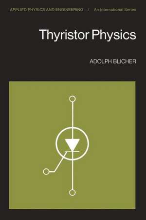
Thyristor Physics: Applied Physics and Engineering, cartea 12
Autor A. Blicheren Limba Engleză Paperback – 12 dec 2011

Preț: 377.94 lei
Puncte Express: 567
Carte tipărită la comandă
Livrare economică 18 noiembrie-02 decembrie
Livrare prin curier în România Termenul estimat este afișat lângă disponibilitate.
Transport gratuit de la 400.00 lei Plată online sau ramburs, în funcție de opțiunile comenzii.
Retur gratuit în 14 zile Comandă securizată și suport în română.
Specificații
ISBN-13: 9781461298793
ISBN-10: 1461298792
Pagini: 324
Ilustrații: XVI, 303 p.
Dimensiuni: 155 x 235 x 18 mm
Greutate: 0.49 kg
Ediția:Softcover reprint of the original 1st ed. 1976
Editura: Springer
Colecția Applied Physics and Engineering
Seria Applied Physics and Engineering
Locul publicării:New York, NY, United States
ISBN-10: 1461298792
Pagini: 324
Ilustrații: XVI, 303 p.
Dimensiuni: 155 x 235 x 18 mm
Greutate: 0.49 kg
Ediția:Softcover reprint of the original 1st ed. 1976
Editura: Springer
Colecția Applied Physics and Engineering
Seria Applied Physics and Engineering
Locul publicării:New York, NY, United States
V-ar putea interesa
-
 Engineering: A Very Short IntroductionDavid Blockley-20%Preț: 56.81 lei71.01 lei
 -
 Posteriori Error EstimationAinsworth-9%Preț: 1207.35 lei1326.76 lei
 -
 Bolton, W: Engineering ScienceWilliam Bolton-23%Preț: 196.66 lei256.32 lei
 -
 -19%Preț: 494.54 lei610.54 lei
 -
 Architecture and Principles of Systems EngineeringCharles Dickerson-18%Preț: 1026.53 lei1251.87 lei
 -
 The Art of Systems ArchitectingMark W. Maier-20%Preț: 946.52 lei1183.15 lei
 -
 Topografa de ObrasIgnacio Corral Manuel De VillenaPreț: 298.57 lei
Public țintă
ResearchCuprins
1 Device basics.- 1.1 Introduction.- 1.2 SCR current-voltage characteristics.- 1.3 Basic SCR construction features.- 1.4 Gate triggering.- 1.5 Holding current.- 1.6 Triggering a shorted emitter SCR.- 2 Current Gain.- 2.1 Variation of current gain with current.- 2.2 Current gain measurement.- 3 Thyristor Maximum Voltage Blocking Capability.- 3.1 Introduction.- 3.2 Maximum forward-blocking capability VBO.- 3.3 Maximum reverse-blocking capability.- 3.4 The punch-through condition.- 3.5 Temperature dependence.- 3.6 Surface breakdown.- 3.7 Reverse-conducting thyristor.- 4 Some High-Injection-Level Effects.- 4.1 Introduction.- 4.2 Ambipolar mobility and diffusivity.- 4.3 Mobility and diffusivity versus current density.- 4.4 Lifetime at high injection levels.- 4.5 High-low junctions at high current densities.- 4.6 Current gain fall-off.- 5 The Gate-Triggered SCR Turn-On Transient.- 5.1 Introduction.- 5.2 Charge-control model of a bipolar transistor.- 5.3 Charge-control model of a p-n-p-n structure.- 5.4 Delay time.- 5.5 Rise time with a resistive load.- 5.6 Rise time with inductive load.- 5.7 Propagation of the on state.- 6 The Nongated, Undesirable Thyristor Triggering.- 6.1 Introduction.- 6.2 Thermal turn on.- 6.3 Light triggering.- 6.4 Voltage triggering.- 7 Thyristor Voltage Drop in the On State.- 7.1 Introduction.- 7.2 Herlet’s closed-form p-i-n diode analysis.- 7.3 Kokosa’s numerical analysis.- 7.4 Numerical analysis of Cornu and Lietz.- 7.5 Otsuka’s forward-drop analysis.- 8 SCR Turn-off Transient.- 8.1 Introduction.- 8.2 Storage time ts1.- 8.3 Fall time tf1.- 8.4 Storage time ts2.- 8.5 Fall time tf2.- 8.6 Effect of the gate current.- 8.7 Simplified approaches.- 8.8 Experimental data.- 9 Gate Turn-off Thyristor (GTO).- 9.1 Introduction.- 9.2 Plasma-pinchingmechanism.- 9.3 Turn-off velocity.- 9.4 Pinching (focusing) time and turn-off gain.- 9.5 Maximum anode and gate currents.- 9.6 Plasma-pinching in the ungated n base.- 9.7 Theoretical model compared with experiment.- 10 Thyristor di/dt and Current Pulse Capability.- 10.1 Introduction.- 10.2 Test circuit for gate-triggered di/dt.- 10.3 Initial turn-on region.- 10.4 di/dt capability of the gated and nongated turn on.- 10.5 Localized temperature rise for a short single pulse.- 10.5 Temperature rise for long or recurrent pulses.- 10.7 Temperature rise and transient thermal impedance during turn-on spreading.- 10.8 Methods of increasing the initial turn-on area.- 10.9 Emitter gate.- 10.10 Emitter shorts versus the turn-on time.- 10.11 Beam-fired thyristor.- 10.12 Field-controlled thyristor.- 11 Bidirectional p-n-p-n Switches.- 11.1 Introduction.- 11.2 Bidirectional p-n-p-n diode switch.- 11.3 Current distribution across a forward-biased junction bounded by resistive layers (current-crowding effect).- 11.4 Junction gate.- 11.5 Remote gate.- 11.6 Triac.- 12 Commutation of Triacs.- 12.1 Introduction.- 12.2 Current and voltage waveforms during commutation.- 12.3 Role of stored charges in triac commutation.- 12 A Recovery of a p+ -n abrupt-junction diode.- 12.5 Snubber networks for dv/dt suppression.- 13 Silicon Surface.- 13.1 Introduction.- 13.2 Ideal MOS diode.- 13.3 Silicon surf ace states and charges.- 14 Avalanche Breakdown Enhancement by Mesa Contouring.- 14.1 Introduction.- 14.2 Positive and negative bevel angles.- 14.3 Theoretical approach to the field computation in the depletion region.- 14.4 Negative bevel angle.- 14.5 Positively beveled junctions.- 14.6 Novel approaches to beveling.- 15 Planar-Junction Avalanche Breakdown Improvement.- 15.1 Introduction.- 15.2 Diffused guard ring.- 15.3 Junction field plate, annular ring, and channel stopper.- 15.4 Resistive field plate.- 15.5 p-n junction with field limiting rings.- 15.6 Etch-contoured planar junctions.- 16 Thyristor Thermal Response.- 16.1 Introduction.- 16.2 Heat generation and absorption in the forward-biased thyristor.- 16.3 Determination of junction temperature.- 16.4 Generalized concept of thermal impedance.- 16.5 Device temperature response to an arbitrary power waveshape.- 16.6 Thyristor thermal impedance measurement.- 16.7 Computer-aided thermal analysis.- 17 Thyristor Circuits Basics.- 17.1 Introduction.- 17.2 SCR and triac control and triggering methods.- 17.3 Thyristor triggering devices.- 17.4 Commutation.- 17.5 Effect of an impedance between the gate and cathode of a thyristor.- 17.6 Thyristor protection circuits.- 17.7 Some thyristor applications.