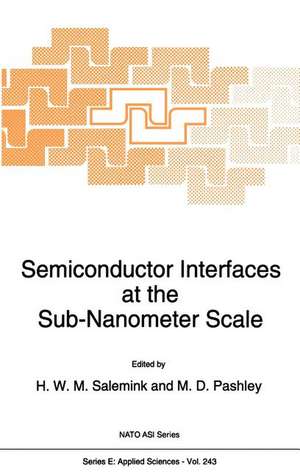
Semiconductor Interfaces at the Sub-Nanometer Scale: NATO Science Series E:, cartea 243
Editat de M. D. Pashley, H. W. M Saleminken Limba Engleză Hardback – 31 iul 1993
Din seria NATO Science Series E:
- 18%
 Preț: 983.83 lei
 - 18%
 Preț: 1905.37 lei
 -
 Preț: 374.84 lei
 -
 Preț: 386.34 lei
 - 20%
 Preț: 349.72 lei
 -
 Preț: 408.17 lei
 - 18%
 Preț: 1262.17 lei
 - 18%
 Preț: 1895.10 lei
 - 18%
 Preț: 1758.89 lei
 - 18%
 Preț: 1267.94 lei
 -
 Preț: 368.86 lei
 -
 Preț: 393.75 lei
 - 18%
 Preț: 1898.69 lei
 - 18%
 Preț: 1761.90 lei
 - 5%
 Preț: 355.87 lei
 -
 Preț: 391.71 lei
 -
 Preț: 412.56 lei
 -
 Preț: 388.01 lei
 -
 Preț: 387.28 lei
 - 18%
 Preț: 3138.09 lei
 -
 Preț: 377.01 lei
 - 5%
 Preț: 376.18 lei
 - 18%
 Preț: 1267.94 lei
 - 18%
 Preț: 1268.37 lei
 - 18%
 Preț: 1273.50 lei
 - 5%
 Preț: 3393.87 lei
 - 18%
 Preț: 1898.48 lei
 - 5%
 Preț: 367.92 lei
 - 18%
 Preț: 1266.27 lei
 -
 Preț: 382.33 lei
 -
 Preț: 384.16 lei
 - 18%
 Preț: 2569.38 lei
 - 5%
 Preț: 1474.32 lei
 -
 Preț: 384.40 lei
 - 5%
 Preț: 2211.40 lei
 - 18%
 Preț: 1903.71 lei
 -
 Preț: 388.20 lei
 -
 Preț: 398.39 lei
 -
 Preț: 402.06 lei
 - 20%
 Preț: 331.65 lei
 - 18%
 Preț: 979.10 lei
 - 18%
 Preț: 1268.99 lei
 - 20%
 Preț: 1974.01 lei
 - 20%
 Preț: 2105.96 lei
Preț: 1259.51 lei
Preț vechi: 1535.98 lei
-18%
Puncte Express: 1889
Carte tipărită la comandă
Livrare economică 04-18 decembrie
Livrare prin curier în România Termenul estimat este afișat lângă disponibilitate.
Transport gratuit pentru acest produs Plată online sau ramburs, în funcție de opțiunile comenzii.
Retur gratuit în 14 zile Comandă securizată și suport în română.
Specificații
ISBN-13: 9780792323976
ISBN-10: 0792323971
Pagini: 272
Ilustrații: XI, 256 p.
Dimensiuni: 160 x 241 x 20 mm
Greutate: 0.52 kg
Ediția:1993
Editura: SPRINGER NETHERLANDS
Colecția NATO Science Series E:
Seria NATO Science Series E:
Locul publicării:Dordrecht, Netherlands
ISBN-10: 0792323971
Pagini: 272
Ilustrații: XI, 256 p.
Dimensiuni: 160 x 241 x 20 mm
Greutate: 0.52 kg
Ediția:1993
Editura: SPRINGER NETHERLANDS
Colecția NATO Science Series E:
Seria NATO Science Series E:
Locul publicării:Dordrecht, Netherlands
V-ar putea interesa
-
 A Treatise on Electricity and Magnetism: Volume 2James Clerk Maxwell-26%Preț: 392.00 lei532.80 lei
 -
 Surface Electronic Transport Phenomena in SemiconductorsV. N. Dobrovolsky-19%Preț: 300.11 lei369.61 lei
 -
 Synchrotron Radiation: Production and PropertiesPhilip Duke-27%Preț: 342.31 lei467.52 lei
 -
 Physics of Ferromagnetism 2eSoshin Chikazumi-24%Preț: 569.20 lei745.21 lei
 -
 Molecular Electromagnetism: A Computational Chemistry ApproachStephan P. A. Sauer-24%Preț: 613.94 lei806.28 lei
 -
 Magnetism: A Very Short IntroductionStephen J. Blundell-20%Preț: 56.97 lei70.82 lei
 -
 Electricity and Magnetism, Volumes 1 and 2B. I. Bleaney-23%Preț: 603.75 lei786.29 lei
 -
 MagnetismDerek J Craik-9%Preț: 844.72 lei928.27 lei
 -
 Electricity, Relativity and MagnetismDerek J Craik-9%Preț: 2951.49 lei3243.40 lei
 -
 Modern ElectrodynamicsAndrew Zangwill-8%Preț: 543.17 lei590.40 lei
 -
 Classical Electromagnetism in a NutshellAnupam Garg-19%Preț: 742.91 lei917.17 lei
 -
 The Manga Guide to ElectricityKazuhiro Fujitaki-18%Preț: 140.38 lei172.15 lei
 -
 Electromagnetic Theory, Volume 3Oliver HeavisidePreț: 180.41 lei
Public țintă
ResearchCuprins
I. Epitaxial Growth of Semiconductors.- “Surface Atomic Processes during Epitaxial Growth”.- “Formation Mechanism of CuPt-Type Sublattice Ordering for III-III-V Type Compound Semiconductors”.- “Surface Chemistry in the Si/Ge GSMBE System Studied Using RHEED”.- “Diffusion of Si in ?-Doped GaAs Studied by Magneto Transport”.- “Theory of Atomic-Scale Processes during Epitaxial Growth: Current Status”.- “A Comparison of Growth by Molecular Beam Epitaxy, Metalorganic Chemical Vapour Deposition and Chemical Beam Epitaxy”.- “The Role of Surface Reconstructions in MBE Growth of GaAs”.- “A Lattice Gas Analysis of Binary Alloys on a Tetrahedral Lattice”.- “Resonant Tunnelling via the Bound States of Shallow Donors”.- II. Electronic Properties of Semiconductor Interfaces.- “Engineering of Semiconductor Heterostructures by Ultrathin Control Layers”.- “Interface Chemical Structure, Band Offsets and Optical Properties of Various III-V Compounds Heterostructures”.- “Dipole Layers at GaAs Heterojunctions and Their Investigation”.- “Clustering and Correlations on GaAs-Metal Interface”.- III. Atomic Scale Analysis of Semiconductor Interfaces.- “Cross-Sectional Scanning Tunneling Microscopy of GaAs Doping Superlattices: Pinned vs. Unpinned Surfaces”.- “Semiconductor Interfaces: Structure, Properties and Processing at the Atomic Level”.- “Epitaxial Interfaces of III-V Heterostructures: Atomic Resolution, Composition Fluctuations and Doping”.- IV. Group IV Materials.- “Group IV Strained Layer Systems”.- “MISFIT Accommodation during Heteroepitaxial Growth”.- “Smear-Out of the Ge/Si Interface in Gas Source MBE Monitored by RHEED”.- “Optical Properties of Imperfect Si-Ge Heterostructures”.- “Si1-x-yGexCy Growthand Properties of the Ternary System”.- “Atomic-Scale View of Epitaxial Layers with Cross-Sectional Scanning Tunneling Microscopy”.- V. Nanometer Scale Devices.- “Atomic-Scale Understanding and Controllability of Heterointerfaces in Quantum Microstructures”.- “Do Periodic Interface Corrugations Cause the Unusual Optical Properties of GaAs/AlAs Heterostructures Grown on Non-(100)-Oriented Substrates?”.- “Strained Layer Quantum Well Semiconductor Lasers”.- List of Participants.